
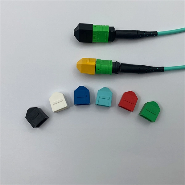
Nigeria Sfp Optical Module Suppliers Directory provides list of Nigeria Sfp Optical Module Suppliers & Exporters who wanted to export sfp optical module from Nigeria. Don't know your target market? Wanted to market your Sfp . The Cisco SFP 10G SR module is meant to provide data transfer at 10Gbps speed with short-range. Qsfp-100g-sr4-s 100g sfp module s-class qsfp-100g-sr4-s 100gbase sr4 qsfp transceiver, mpo, 100m. Small Form-factor Pluggable (SFP) is a compact, hot-pluggable network interface module format used. The best choice is Cisco SFP Transceivers are the best in offering high performance and flexibility in the enterprise and data center networking. The hot-swap modules offer speeds of 1G, 10G, 25G, 40G, and 100G and will smoothly scale to various networking requirements. They come in SFP+, SFP. Fiber optic transceivers are widely used in telecommunication, CATV, FTTx, and various kinds of other data communications. Their commitment to high-quality service and tailored recommendations can support organizations looking to enhance their digital operations. Do You Really Know Where Your Transceivers Come From? Factory-direct optical transceivers and high-speed cables, from legacy links to 1. 6T, built to deploy faster, scale cleaner, and stay compatible as your network evolves. At scale, the biggest problems come from what you don't control, not what.
[PDF]
China is scaling domestic capabilities, with TeraHop*, Hisense, Accezlink, amongst others, shipping millions of modules to power AI interconnects. The global silicon photonics market is projected to reach $9. 2 billion by 2028, with a CAGR of 19. 4% from 2023 to 2028. Asia Pacific is expected to grow at a CAGR of 22. 1% from 2023 to 2028, driven by data center. The increasing adoption of cloud computing, artificial intelligence, and machine learning necessitates more efficient and scalable optical interconnects, where silicon photonics offers a compelling solution due to its cost-effectiveness, miniaturization, and CMOS compatibility. 4% CAGR during the forecast period (2025-2031). Silicon photonics is experiencing strong growth due to the increasing demand for high-speed data transmission in AI, cloud computing. Yole Group unveils its latest photonic market and technology analyses, Silicon Photonics 2025 and Co-Packaged Optics for Data Centers 2025, which explore how AI-driven demand is reshaping connectivity, from transceivers to packaging innovation. 200G/channel will become the new mainstream, enabling. GlobalFoundries (GF) reported fourth-quarter 2025 revenue of $1. 83 billion and highlighted silicon photonics, advanced packaging, and GaN power as central growth engines tied to AI data center buildouts. Communications infrastructure and data center revenue rose 32% year-over-year in Q4 and 29% for.
[PDF]

In this study we consider a basic mechanism for the conversion from Sol. Energy to power generation and the progress in PV development by using silicon materials. Modules based on c-Si cells account for more than 90% of the photovoltaic capacity installed worldwide, which is why the analysis in this paper focusses on this cell type. This study provides an overview of the current state of silicon-based photovoltaic technology, the direction of. The U. Department of Energy (DOE) Solar Energy Technologies Office (SETO) supports crystalline silicon photovoltaic (PV) research and development efforts that lead to market-ready technologies. 7 × 10 17 W of Sol. Energy irradiates the Earth, which is more than 10,000 times the global energy consumption [6, 7]. Conventional PV cells are made from a silicon wafer that transforms sunlight directly into electricity. These silicon-based solar cells use 150 to 200. Crystalline silicon (c-Si) photovoltaics has long been considered energy intensive and costly. Over the past decades, spectacular improvements along the manufacturing chain have made c-Si a low-cost source of electricity that cannot be ignored anymore. Over 125 GW of c-Si modules have been.
[PDF]

Lasers, modulators, and photodiodes form the core architecture of optical transceivers, enabling light-speed communication across global networks. Lasers generate the optical carrier. Modulators encode digital information. The choice of laser directly influences a transceiver's distance, data rate, and reliability. What Is an Optical Modulator? A modulator encodes electrical signals onto the laser's light, controlling properties such as intensity, phase, or polarization to represent digital data. It acts as the. Optical modules are compact devices that convert electrical signals into optical signals and vice versa. These modules typically consist of a laser or LED transmitter, a. In the digital age, optical communication technology is evolving at an astonishing speed, and coherent optical modules, as its core components, are leading the transformation from 5G to AI data centers. In 2025, with the explosive growth of global data traffic, the market size of coherent optical. The optical module serves as a crucial component in optical fiber communication systems, operating at the physical layer, which is the lowest layer in the OSI model. Operating at the physical layer of the OSI model, optical modules are core devices in optical. That is, metal medium communication represented by coaxial cables and network cables is gradually being replaced by optical fiber media. Composition of Optical Modules The optical module, known as Optical Transceiver in.
[PDF]
This chapter presents the development of the Energy Internet throughout the history as an evolutionary solution based on modern technological development and needs, with the respect of its architecture, key features, and key concepts, such as energy router, prosumer, and virtual. This chapter presents the development of the Energy Internet throughout the history as an evolutionary solution based on modern technological development and needs, with the respect of its architecture, key features, and key concepts, such as energy router, prosumer, and virtual. Energy Internet is a concept proposed to harness, control, and manage energy resources effectively, with the help of information and communication technology. The. Therefore, a new energy paradigm is known as the “Energy Internet” that combines economics, energy, and technology in an open, equal, and coordinated fashion. Energy Internet (often reflects Internet plus energy) is a novel energy network that interconnects the power system components: production. Similar to an internet router to connect and switch networks, the energy router within the energy internet plays a crucial role to integrate and distribute the energy flow. This paper provides an overview of the application and challenges associated with energy routers in the energy internet.
[PDF]

This article summarizes the research and development of a fully automated production process for optical fiber couplers, covering stages from fiber loading to glue packaging, which was demonstrated through the creation of a prototype and is expected to improve mass production . This article summarizes the research and development of a fully automated production process for optical fiber couplers, covering stages from fiber loading to glue packaging, which was demonstrated through the creation of a prototype and is expected to improve mass production . A fiber coupler is a passive optical device that manages the flow of light signals within an optical network. It functions by dividing a single incoming light path into multiple outgoing paths, or by combining light from several input paths into a single output fiber. They form the foundation of high-speed communications, ensuring that data, sensor signals, and laser outputs reach their destinations with minimal loss. Beyond simple. Fiber optic coupler is a lively type of passive components, and its basic function would be to achieve the optical power and fiber wavelength distribution.
[PDF]
It essentially performs some relatively simple time-division multiplexing of lower-rate signals into a higher-rate carrier within the system (a common example is the ability to accept 4 OC-48s and then output a single OC-192 in the 1,550 nm band).OverviewIn, wavelength-division multiplexing (WDM) is a technology which a number of signals onto a single by using different (i.e., colors) of. A WDM system uses a at the to join the several signals together and a at the to split them apart. With the right type of fiber, it is possible to have a device that does both s.
[PDF]

Companies like Tesla, CATL, and Fluence are deploying battery farms that can store megawatts of solar power and release it on demand. Meanwhile, “smart grids” enabled by AI and real-time data are helping to balance supply and demand dynamically. Energy Internet technology promotes the deep integration of energy and communication infrastructure and creates an open and shared Internet ecosystem. The energy Internet theory has been not only applied to the industrial field but also developed to be used in the agricultural field (Fu and Yang. From the first fires that lit our ancient caves to the towering smokestacks of the Industrial Revolution, each leap forward in power generation has redefined how we live, work, and relate to the planet. But the fossil fuel era—so dominant, so defining—is reaching its inevitable twilight. The signs. ITM University Gwalior, India. coordinating and controlling the many parts of a system, whether they are locally located or geographically dispersed. The study wraps up by outlining the most pressing problems that will need to be solved in order to implement an.
[PDF]

Also, please take a look at the list of 18 fiber optic sensor manufacturers and their company rankings. Omega Engineering, Inc. What Is a Fiber Optic Sensor?. The top companies in distributed fiber optic sensors market are shaping a rapidly evolving ecosystem driven by infrastructure digitization, energy transition, and advanced monitoring requirements across critical industries. The market is estimated to exceed USD 2. Their systems offer a compelling combination of advanced technology (often utilizing Brillouin or Rayleigh scattering). Fiber optic sensor companies manufacture sensors that use optical fibers for detecting changes in physical properties like temperature, pressure, and strain. The technology is developed at the VU in Amsterdam they built several applications based on the technology, for both academic as well as. com/ Echopoint Medical is a. Fiber optic shape sensing platforms delivering full-length device awareness for radiation-free navigation and real-time procedural insight What is Shape Sensing? Fiber optic shape sensing uses embedded sensors to measure the full 3D shape of a flexible surgical device along its entire length in.
[PDF]

This order establishes the program, planning, and implementation guidelines for upgrading communication systems that support the National Airspace System (NAS) at major airports. Our mission is to be your innovative development partner providing cost effective solutions for subsea use. We are a small team backed by decades of experience, combining different skills, backgrounds, and expertise: From sales, through engineering, manufacturing, testing and service, we. For over two decades, we have delivered tailored fiber optic solutions to Norway's most demanding projects. NFO Engineering specialize in offshore and maritime fiber optics, as well as complex infrastructure solutions for tunnels, data centers, and node construction. Through our expertise we ensure. IHSE's high performance KVM extenders and matrix switches bring new levels of functionality and capability to air traffic and airport operations. When we were established in 2001, we were among the first companies in Norway to specialize in fiber optics. Communication systems are herein defined to include discrete control/monitor, digital data, voice/voice frequency, and. N0r5ke Fibre is a Norwegian digital infrastructure company, founded by Norwegian entrepreneurs Anders and Bjørn Vik. As a neutral and independent company we lease.
[PDF]

Compared to conventional metallic cables, optical fiber provides an advantage of low loss (~ 0. 2dB/km) and wide bandwidth (several hundred MHz to THz) to enable long-distance, high-capacity communication. Fiber-optic communication is a form of optical communication for transmitting information from one place to another by sending pulses of infrared or visible light through an optical fiber. The light is a form of carrier wave that is modulated to carry information. Fiber is preferred. It was almost a century later before optical-based communication was put to practical use, thanks in large part to the invention of optical fiber and lasers. A laser's stable, highly directional beam of light (emitted from tiny semiconductor windows that measure just a few hundred thousandths of a. In 2020, we celebrated the 50th anniversary of the invention of low-loss optical fiber — an innovation that has transformed the way we connect and that lies at the cornerstone of our communications revolution. In a Corning lab on a Friday afternoon five decades ago, a single strand of glass and a. Fibre optics and optical communications is the use of thin strands of glass for sending information encoded into light over long distances. Total internal reflection prevents light inserted into one end of the fibre from escaping through the sides. Transferring information optically in this way.
[PDF]

We presented a highly efficient 1×3 optical power splitter based on photonic crystal waveguides (PCWs) with a triangular lattice of air holes. By only modifying a single hole in a Y junction area, the input power can be almost evenly split into three ports. In this paper, we present various designs of optical splitters for access networks, such as GPON and XG-PON by ITU-T with triple-play services (ie data, voice and video). The presented designs exhibit a step forward, compared to the solutions recommended by the ITU, in terms of performance in. Optical Line Terminal Equipment (OLTE), Optical Network Unit (ONU), Erbium-Doped Fiber Amplifier (EDFA), Asynchronous Digital Subscriber Line (ADSL), Very High-Speed Digital Subscriber Line (VDSL) The technical paper explains in detail about the basic design & implementation of Triple play service. A fiber optic splitter is a passive optical component that divides a single incoming optical signal into two or more outgoing signals, or combines multiple incoming signals into one. The optimal device can operate with a. To provide a unified business, we must have a network platform that can support various multimedia (streaming) business such as audio and video. The characteristics of these businesses are large business demand, large data volume, and high service quality requirements. Therefore, it is generally. problematic when the number of requests in an area with a demand that vertical building in an area.
[PDF]
HDPE Silicon Core Pipe is a high-performance conduit specially designed for optical cable protection. Featuring a durable HDPE outer layer and a low-friction silicon inner lining, it enables smooth and long-distance cable installation in telecom, internet, and infrastructure projects. In this. Qitian Communication Industry Ningxia Co., Ltd is a well-known supplier of communication pipeline and related supporting products., was established in 2006. Over the years, we have been dedicated to providing solutions for high-speed. Home / Library / Public Doc / Product Specification Sheets NEED A CUSTOM QUOTE? Work with our experts to build the best solution for your environment. Email us using the Request a Quote below, or. Established in 2007, the 50,000sqm Jiajie Manufacturing Base owns the most advanced automatic production lines in China to reach volume production capacity up to 60tons/month, ranking the frontline in the world. One-stop Service / Your satisfaction, our motivation. Material: PE 80, PE 100 2. Size: 32/26, 34/28, 40/33,46/38, 50/41, 63/54 3. CO (Certificate of Origin): China, CO could be provided by free. MOQ: Trial Order or 1*20ft containers by. Optical Fiber Core could be applied as G. A2, OM1, OM2, OM3, OM4 according to needs. Maximum Tensile Strength could be changed according to technical demand. Standard: TS EN 60794 +20 C -20 C +70 C +20 C -Number of cycles: 2 turns -Time per each step: 12 hrs.
[PDF]
